MEMS
Resonant Microsensors
UETP-MEMS Course: Resonant microsensors
- Thomas Fabula, Hans-Joachim Wagner, Institute of Microstructure and Information Technology (IMIT), Villingen-Schwenningen, Germany
- Albert Prak, MESA Research Institute, University of Twente, Enschede, the Netherlands
Introduction to MEMS and resonant sensors
1.1 Micro-electro-mechanical-systems
The capability of microelectronics has been increased about more than thirty years concerning geometrical size, power consumption and access time of the miniaturized electronic devices. The overall performance was increased by about ten dimensions, leading to numerous new applications and an increasing use of microelectronics in every field of modern life. Though the potential of new electronical applications is not yet exhausted it seems, that a further penetration of microelectronics into new products is beeing hampered by the lack of miniaturized sensors and actuators. There is a great demand for silicon based sensors and actuators which are able to master the tasks of automatic, multidimensional data acquisition and process control. To be comparable with the world of microelectronic devices, sensors and actuators must be fabricated with a similar technology leading to comparable driving voltages, dimensions, complexity and prize.
The advantages of Micro-electro-mechanical-systems (MEMS) are found in the five technical dimensions [1.2]: availability of materials, possibility of miniaturization, realization of complex arrangements, system integration with microelectronics and use of the whole width of physical phenomena. To build MEMS silicon plays as material a dominant role. Its elastical and mechanical properties are comparable to those of steel, whereas the density can be compared with aluminium. Thermal conductivity is comparable with molybdenum and wolfram. The structural perfection of grown monocrystals of silicon is nearly ideal. Other materials like germanium, quartz and gallium‑arsenide can also be used for micromechanics and/or for special devices. Additionally, a great number of thin film materials can be deposited with very small pollutions by the various methods of the microelectronic technology (see chapter 2).
Miniaturization is the most important key aspect of MEMS. Already in 1959 Richard Feynman pointed out in his talk ‘there’s plenty of room at the bottom’ [1.3] the possibilities of miniaturization and gave some interesting aspects on ‘what is small’. One of the main differences in manufacturing devices by precision mechanics or by microtechnology is the use of photolithography and etching techniques to perform MEMS. By this means the minimum structure width can be in the submicron range for bulk micromachined devices, typical size dimensions are in the order of some hundred microns. These dimensions are small enough to take advantages from reduced size, reduced mass and reduced volume.
Most of the todays applications for MEMS are a 1:1 replacement of precision mechanical sensors. But in the near future it is expected that with complex arrangements of MEMS the main costs of a sensor system may be reduced drastically. On the other hand multifunctional sensor arrays may be constructed, which perform with increased accuracy and reveal greater redundancy (e.g. array of cantilevers performing a multisensor for vibration measurements, array of pressure sensors for tactile applications). Because of the multifunctionality the sensor elements can be standardized and `personalized’ by software. By means of this, overhead and storage costs can be reduced, and the total costs are additionally lowered by higher production volumes.
System integration with microelectronics will facilitate smart sensors and actuators with the possibility of on‑chip microelectronics and control functions (example: integrated acceleration microsensor ADXL50 from Analog Devices with digital on-chip electronics). In the case of silicon based sensors and actuators it seems not to be a problem to integrate microelectronic bipolar or MOS devices on the chip. A problem to be solved may be the process compatibility of microelectronical and micromechanical processes. Micromechanical devices with integrated on-chip electronics should be direct adressable by a data bus and only relevant information will be given to a central computer. Systems build up with smart sensor and actuator devices should be safer, faster and more reliable. At the moment the tendency is more to a hybride system configuration, because of the problem of process compatibility and because there are not yet a large number of high volume sensors and actuators requiring a specialized on-chip electronics.
Micromachined structures can be combined with a great number of physical phenomena. There are numerous applications in combination with microoptics, where diffracting structures or bending gratings can take over the static distribution of information fluxes. Combined with magnetism, micromachined magnetic heads detect data from magnetic discs or SQUIDs (superconducting-quantum-interference-devices) take information of celebral currents. Thermodynamic phenomena like thermal conductivity, diffusion or evaporation in combination with micromachined shapes can lead to disposes showing new effects, which could not be realized before [1.4]. There are chemical and biochemical sensors under development, which can detect the concentration of a specific gas within a mixture of many gas species or which are able to realize direct imuno-assays. Especially microresonators with non-selective or selective adsorbing layers are suitable to construct gravimetric chemical and biological resonant sensors [1.5].
Considering the advantages of MEMS there is the question, why MEMS as industrial products are not available. One of the reasons may be the expensive and long term development of complex arrangements. But also for simple sensors and actuators, a housing is necessary. With the same housing costs the profit is lowered if one is going from precision mechanics to micromachining. There is a great number of possible and (at a research level) realized applications of micromechanics. It is asumed, that the driving force for new products will be the advanced production technology. Mass markets, e.g. the automotive market, will bring micromechanics into industrial products with high volumes and high demands.
There are quite reasonable market forecasts that a great number of miniaturized control devices to be introduced in the coming years will be micromechanical. Considering the present trend on integration of electronical functions into micromechanical devices, the advantages of micromechanics become even more pronounced. There is obviously no other technology with comparable technical and cost advantages to be seen. The biggest market segment is the automotive industry, followed by household, consumer and medical applications. Especially micromechanical sensors are needed in large quantities although the future demand for microactuators should not be neglected. From the view of development advanced types of devices are of even more importance. Quantitative market data for microdevices were published from NovaSensors [1.6] and are based on four market forecasts (MIRC, VDC, Frost & Sullivan, McIntosh). Other market forecasts were made from Battelle (1987, 1992) and Prognos (1992), but the data given from NovaSensors are proven more or less.
1.2 Resonant sensors
Beside other sensor principles resonant sensors are one of the mostly used techiques in sensor applications featuring several advantages. Under a resonant sensor we will understand a device with an element vibrating at resonance which changes its output frequency as a function of the measurand. The frequency domain sensor output is ‘digital’ in the sense that it is basically independent of analog levels and can be connected to digital circuitry [1.7-10]. Also the achievable sensitivities and gauge factors are much greater in contrast to other sensor principles (see chapter 3).
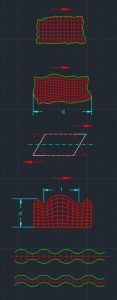
In principle different elastic (or acoustic) waves may be used in microsensor applications which are influenced by the measurand. Elastic waves in solids are dependent on the geometry and the boundary conditions as shown in fig. 1.1. Depending on the excitation conditions longitudinal, transversal or shear Bulk-Acoustic-Waves (BAW) may be excited. Surface-Acoustic-Waves (SAW), which are also called Rayleigh‑waves, just penetrate the surface of the elastic solid, whereas Lamb‑waves or Flexural-Plate-Waves (FPW) occur in very thin plate resonators and force the whole resonator to symmetric or antisymmetric vibrations. In this course we will concentrate mainly on BAW microresonators and will use the synonyme resonant microsensor, because the whole device is vibrating at its resonance frequency. They are fabricated from single crystalline silicon with micromachining technologies, e.g. anisotropic wet etching and thin film deposition, or from single crystalline quartz. Beside bulk-micromachining (BMM) surface-micromachining (SMM) is gaining more importance regarding miniaturization of the resonator devices (realization of resonant strain gauges) and integration of different components in MEMS.
 Fig. 1.1: Different acoustic waves in solids
In resonant silicon sensor applications beams, bridges and diaphragms are often used as resonator elements, which may be operated in different vibrational modes. Excitation and detection of the vibrations is carried out with different operating principles (see chapter 5: PART I and II), but only flexural vibration modes are excitable due to the force or moment excitation mechanism. Because quartz itself is piezoelectric resonant quartz sensors exhibit besides flexural vibration modes a large number of possible other vibration modes, e.g. shear BAW and SH-APW (shear-horizontal acoustic-plate-waves). Beyond physical sensing applications BAW, SAW, FPW and APW devices may be utilized also for chemical sensing [1.11], but these applications will not be considered in this course at all.
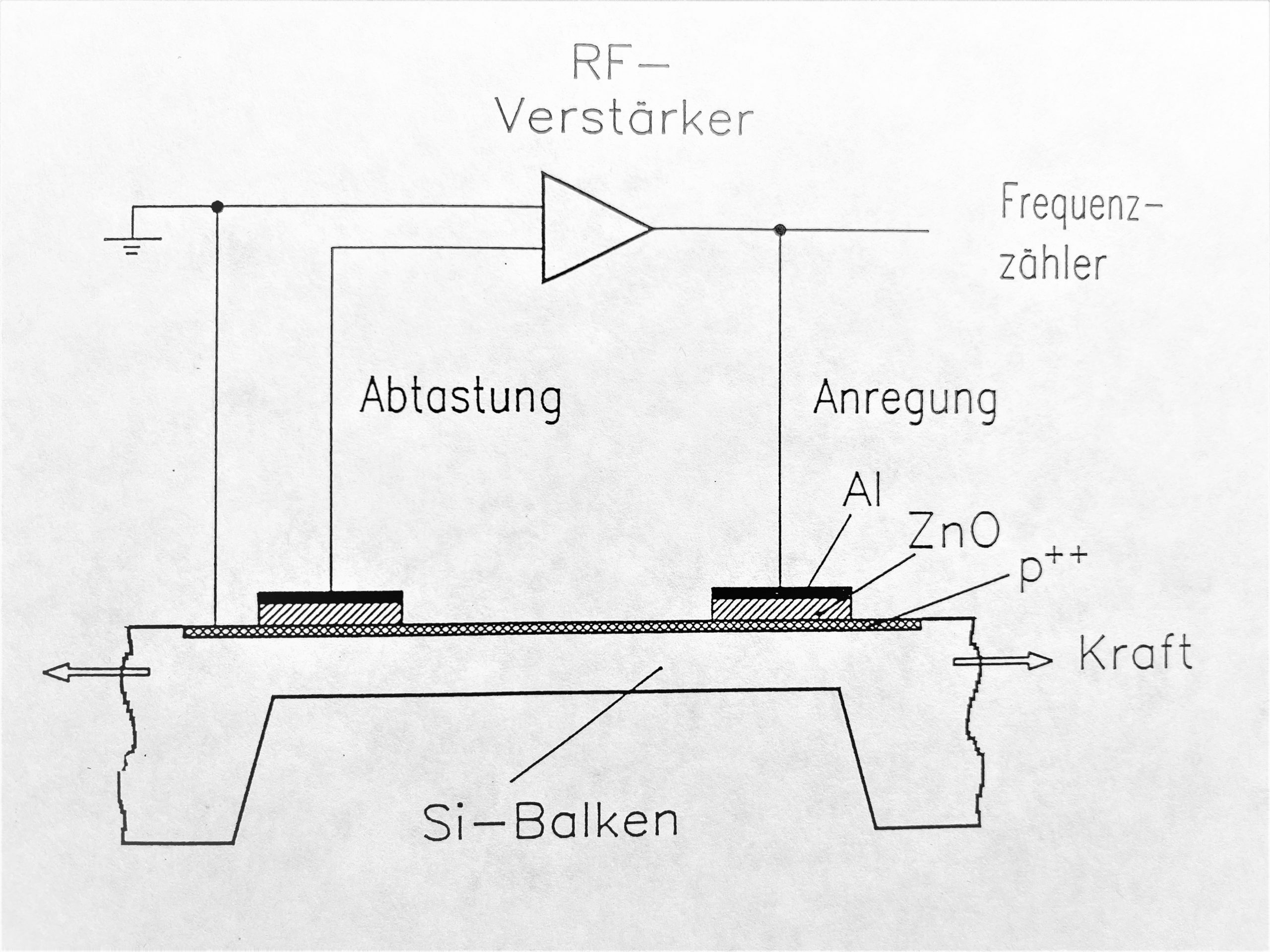
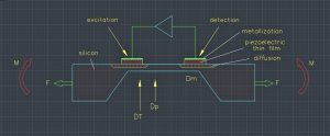
Different sensing mechanisms may be used for sensor applications. In principle the characteristics of an (ultrasonic / acoustic) elastic wave propagating along a path are altered by the measurand. The sensor effect may result in a frequency shift due to the change of the resonators stress state, a phase shift of the elastic wave or an attenuation of the wave amplitude. For physical sensing applications mainly the first effect is utilized. A resonant silicon bulk microsensor for pressure or force measurement is shown schematically in figure 1.2. The sensor is driven to resonant vibrations, e.g. by piezoelectrical thin films. The resonant element consists of a silicon diaphragm or beam wet etched from the backside and in case of a vibrating beam separated from the bulk material via dry etching techniques (e.g. RIE). Piezoelectric thin films (e.g. zincoxide, ZnO) are used to excite and to detect the vibrations of the resonator which is connected to the feedback loop of an oscillator circuit driving the silicon resonator at its mechanical resonance frequency.
Fig. 1.2: Schematic principle of a resonant bulk silicon microsensor
Mechanical loading of the resonator due to a pressure difference at the diaphragm, or axial forces F exerted to the beam, or bending moments M acting on the resonator will result in a tensile stress in the resonator element. On the other hand a temperature rise ΔT will induce compressive stress due to the temperature dependent material properties of the microsensor. Due to the different loads stress stiffening effects will occur and increase/decrease the stiffness of the resonator and change therefore its resonance frequency. The output of the electronic oscillator circuit is fed to a frequency counter registrating the load dependent frequency signal. Most resonant silicon microsensors considered in this course work after this principle and comprise a passive resonator element and additionally active elements for vibration excitation and detection.
1.3 Scope of this course
This course concentrates on resonant microsensors fabricated from silicon (or quartz) and familiarizes with resonant sensor principles and possible applications. It is intended to give a quite comprehensive overview on the topics related to resonant microsensors and to indicate the specific possibilities, technological prerequisites and different problems which may lead to performance degradation of the sensor devices.
Chapter 2 gives an overview on used materials and micromachining technologies for the fabrication of resonant silicon microsensors. Especially the mechanical material properties of single crystalline silicon are discussed and compared with other sensor materials. The key technology processes, like photolithography, wet and dry etching of silicon and the various deposition methods for additional materials is described. To complete the technological overview surface-micromachining and the so-called LIGA-process are addressed.
Chapter 3 deals with the basic physical principles governing the static and dynamic behaviour of resonant microsensors. As an example a prismatic microbridge resonator is used to explain the mathematical description of the sensor behaviour. Several analytical solution techniques like Laplace transforms and modal analysis are shortly summarized which are used to solve the underlying differential equation. The response to axial loads completes this chapter and several topics like beam buckling and gauge factors are treated in principle.
The more theoretical topics of the course are freshed up with practical demonstrations. Different resonant microsensors will be presented and practical demonstration will be given on personal computers. For the analyzed microstructures an exact analytical description is often very difficult or even impossible, so numerical methods like finite element analysis (FEA) is used to study the behaviour of the microsensors. The finite element method (FEM) is widely used for the solution of practical engineering problems, also for the design and numerical modeling of resonant sensors.
In chapter 4 some examples of finite element input codes, i.e. source files (FE-program ANSYS [1.12]) are listed to perform numerical calculations (static analysis: to visualize displacements and stress patterns and modal analysis to compute different mode shapes of a resonant diaphragm sensor). Furthermore, results of some typical applications of static and dynamic analyses for simulating resonant sensors are given.
Excitation and detection relevant effects for resonant silicon sensors are discussed in chapter 5. There are several physical excitation and detection mechanisms to operate the silicon sensor devices. Key aspects are electrical cross-talk, coupling efficiencies and selective-mode-excitation (SME) and –detection (SMD). Furthermore, the magnitude and scaling laws of the excitation forces depending on the different mechanisms are considered.
To characterize the overall performance of resonant microsensors damping related effects on the mechanical and electrical quality factor and the influence of mass loading on the resonance frequency has to be known. Additionally, non-linear effects may encounter if large vibration amplitudes are reached. Also the temperature dependence of the resonance frequency mainly due to thermal dependent material properties and due to the multi-layer composition of the resonators plays an important role and limits the performance of the sensor device.
As a case study all required development steps for the realization of a resonant silicon force sensor are summarized in chapter 7. The computer-based design (mask layout) and the simulation results obtained by FEA are discussed. Furthermore, the whole technological fabrication sequences (e.g. ZnO sputter deposition, wet etching, laser assisted techniques) and the experimental characterization of the sensor device is given. The sensor design is based on a triple-beam resonator driven piezoelectrically by reactive sputtered ZnO thin films.
At the end of the course examples and applications of resonant quartz and silicon sensors are given. A comprehensive review documents the research activities and the ‘state of art’ in the field of resonant microsensors. A brief history of resonant quartz sensors (DETF– and AT-resonators) is given in chapter 8.I and for silicon devices in chapter 8.II, respectively. Although, up to now there are only two commercially available resonant silicon sensors for pressure measurements (DRUCK [1.13], YOKOGAWA [1.14], details in chapter 8.II.1) it is worth to mention that their sensitive elements are quite complex resonators, i.e. butterfly- and H-shaped, which are attached to pressure sensitive diaphragms.
Additionally to this course booklet more general information on micromechanics and microsystem technology may be found in the books of A. Heuberger [1.15], S. Büttgenbach [1.16] and S. Middelhoek [1.17], W. Menz [1.18], respectively. The most important Journals are: Sensors and Actuators (Elsevier-Sequoia), Journal of Micromechanics and Micromachining (Institute of Physics, IOP), Sensors and Materials (MYO, Tokio) and Journal of Micro Electro Mechanical Systems (IEEE). Further topics related to the design and modeling [1.19], technological fabrication process [1.20-21], characterization [1.22-23] and packaging aspects [1.24] of micromechanical devices and MEMS are covered by other UETP-MEMS courses and booklets, respectively.
Demonstrations
- Resonant sensor devices
- Finite-Element-Method
- Numerical modeling of resonant sensors
- Load dependent frequency change
- Thermal behaviour of resonant sensors
- Optimization of a ‘beam-on-diaphragm’ pressure sensor
- PC-based layout and FEA demonstrations
- ANSYS program source listings
References
- [1.1] B. Schmidt, UETP-MEMS Course: Micro actuators, FSRM, Switzerland (1993)
- [1.2] Positionspapier des Fachausschusses Mikrosystemtechnik der VDE/VDI‑Gesellschaft für Mikroelektronik (GME), January 1991
- [1.3] R. Feynman, There’s plenty of room at the bottom, talk given on December 26, 1959, annual meeting of the american physical society at the California Institute of Technology, published in: Miniaturization, H.D. Gilbert, Ed., Van Nostrand Reinhold, New York, NY 10003, reprinted in: J. Microelectromechanical Systems, Vol. 1, No. 1 (1992) 60‑66
- [1.4] R. Feynman, Infinitesimal machinery, talk given on february 23, 1983 at the Jet Propulsion Laboratory, Pasadena CA. Reprinted in: J. Microelectromechanical Systems, Vol. 2, No. 1 (1993) 4‑14
- [1.5] A.J. Ricco, S.J. Martin, R.M. White, Short course for Transducers ’91: Fundamentals of ultrasonic sensors, June 23, San Francisco (1991)
- [1.6] Silicon sensors and microstructures, NovaSensors, September 1988
- [1.7] G. Stemme, Resonant silicon sensors, J. Micromech. Microeng. 1 (1991) 113‑125
- [1.8] R.M. Langdon, Resonator sensors ‑ a review, J.Phys.E: Sci.Instrum., Vol.18 (1985) 103-115
- [1.9] R.T. Howe, Resonant microsensors, Proc. TRANSDUCERS ’87, Digest of technical papers, Tokio, Japan (1987) 843‑848
- [1.10] R.A. Buser, Resonant Sensors, in: Sensors, Volume 7, Mechanical Sensors, eds.: H.H. Bau, N.F. de Rooij, B. Kloeck, VCH Verlagsgesellschaft mbH, Weinheim, FRG (1994) 205‑284
- [1.11] P. Hauptmann, Chemical resonant sensors, Int. Symposium on Environmental Sensing, Berlin, 22-26 June (1992)
- [1.12] Swanson Analysis Systems, Inc., Johnson Road, P.O. Box 65, Houston, PA, USA
- [1.13] DRUCK Ltd., Firetree Lane, Groby, Leicester/GB, data sheets: RPT 100, Resonant pressure sensor (1991)
- [1.14] YOKOGAWA Electric Corporation, Data sheets: DPharp ‑ Differential pressure and pressure transmitter, Tokyo, Japan (1993)
- [1.15] A. Heuberger (ed.), Mikromechanik, Springer Verlag, Berlin (1989)
- [1.16] S. Büttgenbach, Mikromechanik, B. G. Teubner, Stuttgart (1991)
- [1.17] S. Middelhoek, S.A. Audet, Silicon sensors, Academic Press Limited, London (1989)
- [1.18] W. Menz, P. Bley, Mikrosystemtechnik für Ingenieure, VCH Verlagsgemeinschaft mbH, Weinheim, FRG (1993)
- [1.19] H. Pavlicek, G. Wachutka, UETP-MEMS Course: CAD tools for MEMS, FSRM, Switzerland (1993)
- [1.20] B. Kloeck, UETP-MEMS Course: Hands on MEMS, FSRM, Switzerland (1993)
- [1.21] M. Elwenspoek, UETP-MEMS Course: Etching technology, FSRM, Switzerland (1993)
- [1.22] B. Cretin, G. Tribillon, UETP-MEMS Course: Optical methods for measurements in microtechnology, FSRM, Switzerland (1993)
- [1.23] P. Beckmann, W. Dreher, W. Nisch, R. Reichl, UETP-MEMS Course: Surface and interface analysis, FSRM, Switzerland (1993)
- [1.24] G. Staufert, H. Reber, H. Hieber, UETP-MEMS Course: Packaging, FSRM, Switzerland (1993)
Acknowledgement
A course developed by UETP-MEMS (University Enterprise Training Partnership for Micro Electro Mechanical Systems) with the support of the European Programme COMETT – Community Programme for Education and Training in Technology. (C)opyright 1994, UETP-MEMS, FSRM, Switzerland
GitHub repositories


