Published in “Mikroelektronik Band 6 – Fachbeilage Mikroperipherik”.
- Main topic: “Modeling of components of microsystem technology”
- Issue: January / February 1992, Issue 1, p. II
- Author: Dipl.-Phys. Thomas Fabula (complete article version)
Finite Element Modeling in Micromechanics
Preamble
In the scope of the modeling of micromechanical components, the finite element method plays an important role in component simulation and increasingly in the field of process simulation. Increasing complexity of structural geometries, different material compositions and the necessity to take into account the influences of different physical quantities place higher demands on the system design. The solution of these tasks requires the use of appropriate computer-aided numerical simulation methods.
Finite Element Method
The finite element (FE) method has long been used successfully in the field of macroscopic elastomechanics to calculate the mechanical behavior of components. The principle is based on a subdivision of the structural geometry into subregions from which the overall structure is approximated by a discrete mesh. A description of the two- or three-dimensional elements used is given by a problem-adapted mathematical approach for the physical field variables being searched for. The solution of the resulting matrix equations for the corresponding degrees of freedom is done on the element level.
To simplify the calculations, as well as to save computational time and memory requirements, FE models with shell or plate elements are largely chosen based on isotropic material properties and a linear component behavior. Thus, first approximate solutions are obtained. In addition to the choice of FE model parameters, such as element approach, meshing and boundary conditions, the structural behavior can be studied and approximated by varying the geometry and material parameters.
In modeling micromechanical components, the sometimes imprecise knowledge and often difficult measurable access of important material properties represents a significant problem. In addition to the direction-dependent crystal properties (anisotropy) and the temperature dependence of the material data, process-dependent effects, such as mechanical stresses in multilayer systems, must be taken into account. In addition, the elastic moduli of microfabricated thin films, for example, differ considerably from those of the bulk material.
The currently available commercial FE program tools offer only rudimentary capabilities to cover the wide range of modeling requirements. In this paper, some applications of the FE method in the modeling of microsystem technology components are presented, taking into account the problems that arise.
Static FE calculations
The subject of static finite element calculations is the study of structural behavior under stationary loads, where the nature of the loads can vary. Mechanical loads can act directly on the microstructures by application of force or pressure, acceleration (e.g. shock loading) or rotation (centrifugal forces). Taking into account the valid symmetry and boundary conditions (constraints), the component deformations, as well as the occurring mechanical stresses are calculated.
Micromechanical elements, such as membranes, beam and paddle structures, exhibit different, overlapping, nonlinear effects that must be taken into account in the design. For this purpose, FE calculations are a suitable tool, since the flexibility of the method also allows the inclusion of small disturbances.
The three-dimensional device structures, such as membranes, fabricated by an anisotropic wet chemical etching process are defined by the etch stop limiting crystal planes. For <100>-oriented silicon wafers (wafers), inclined {111} planes define the constraint geometry of the components. The type of membrane attachment defined in this way can have a significant effect on the stress state by leading to a shift in the locations of maximum stress concentration. In the case of silicon membranes, which are about half the thickness of the silicon wafers, the stress extrema migrate inward from the outer edge of the membrane by up to 3% of the side length as a result of the flexible restraint.
Geometric nonlinearities occur as a further effect. This refers to a load-dependent stress stiffening caused by the restoring forces as the component load increases. Depending on the ratio of the diaphragm thickness to the side length, these cause significantly less diaphragm deflection at high pressures as a result of positive tensile stresses inside the diaphragm.
The nonlinearity of the deflection-pressure or stress-pressure characteristic is typically several percent at high pressures. To improve the linearity behavior, large diaphragm deflections must be prevented. For this purpose, the diaphragm can be reinforced with a structured center section (Boss diaphragm). Its dimensioning is optimized using three-dimensional FE calculations.
The calculation of the nonlinear model behavior requires an iterative procedure in which the component load is successively increased and the component stiffness must be corrected according to the load condition.
Dynamic FE calculations
Dynamic finite element calculations allow the determination of the natural frequencies and the associated natural modes (modal analysis) of micromechanical structures. Under the application of time-dependent loads, which can be periodic or impulsive, the temporal structural behavior can be calculated.
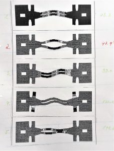
In modal analysis, different vibration modes can arise due to different structural geometries and specific resonator characteristics, such as material properties and boundary conditions. While in the case of silicon membranes only bending vibrations and their harmonics can occur, in the case of quartz membranes superimposed complex vibration modes (e.g. thickness shear vibrations) are also possible due to the crystal structure. In the case of beam resonators, longitudinal and torsional vibrations, as well as superpositions of these vibration modes, can occur in both materials in addition to bending vibrations.
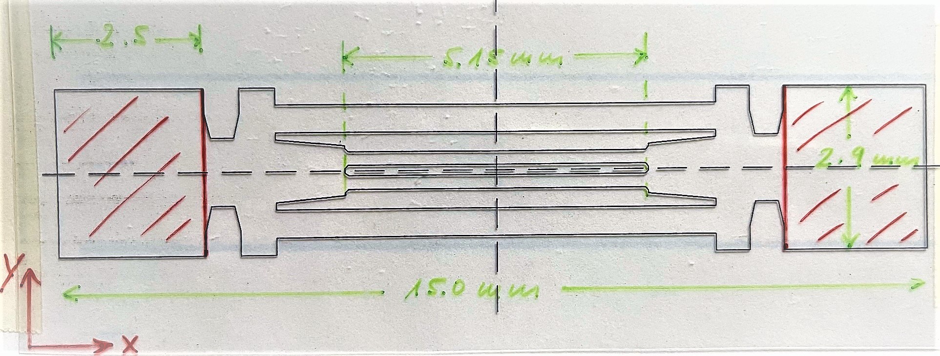
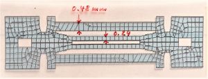
In general, with higher order of the modes, the number of nodes and the probability of superimposed vibration modes increases. The determination of, for example, the bending resonance frequencies of force sensors based on quartz double ended tuning forks (DETF) is already possible with simple, two-dimensional FE model approaches. Deviations from experimentally measured values are less than 2% here.
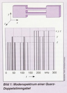
However, the modeling of complex vibration modes requires a three-dimensional formulation, taking into account the anisotropic material behavior. As an example, a typical mode spectrum of a quartz double tuning fork is shown in Fig. 1. In the lower frequency range, different bending vibrations (y-, z-direction) dominate, while with increasing frequency the torsional and superimposed xyz vibrational states increase.
Furthermore, this three-dimensional formulation can be used to study the influences of material and geometry effects. For example, the difference between isotropic and anisotropic material approach for silicon diaphragms leads to a deviation of about 3% for the natural frequencies of the fundamental bending vibrations. Another effect occurs due to the inclined edge restraint in silicon diaphragms and beam resonators, which causes a lowering of the resonant frequencies due to reduced restraint stiffness, which is of about the same order of magnitude.
Beyond the determination of the natural frequencies and modes of vibration, the shift of the resonant frequency as a function of the change of the parameters determining it is of particular interest. This effect can be used to determine a physical parameter and represents the operating principle of frequency analog sensors. The resonant frequency change can be caused, for example, by a mass accumulation or by a change in the mechanical stress in the resonator resulting from a direct application of force or from the influence of temperature.
The calculation of the force-frequency characteristic (force sensitivity) and the temperature sensitivity is performed by a nonlinear, static FE calculation, which is used to determine the change in stiffness of the overall system caused by the measured variable. This can then be used to determine the natural frequencies of the prestressed system.
Furthermore, the load-dependent frequency-force characteristics can be calculated for silicon force sensors with different resonator dimensions. The increase in force sensitivity is associated with an increase in the nonlinearity of the force-frequency characteristics, so that the operating point of the sensor can be suitably adjusted by suitable resonator dimensioning. The temperature-dependent resonant frequency response can be determined using nonlinear, dynamic FE calculations for arbitrary crystal orientations (e.g., quartz oscillators), taking into account the temperature-dependent, anisotropic material properties.
Another consideration in the design of the frequency-analog sensors described above is the selection of the most favorable resonator mounting in order to minimize the structural damping of the oscillator. Depending on the structuring of the resonator mounting, a suitable vibration decoupling can be achieved, resulting in increased vibration quality and improved mode selection (unimodality) of the resonator system.
Frequency response analysis is used to calculate the amplitude spectrum of the natural oscillations, including damping effects, for a time-dependent structural excitation. However, a general problem is the exact knowledge of the individual damping and effective excitation contributions. Therefore, in order to perform appropriate modeling, experimental measurements are required to characterize the dynamic properties of micromechanical components.
Coupled field calculations
Due to the miniaturization and the high degree of integration, components of the microsystem technology show a strong interaction of different physical influence quantities and mostly exhibit unwanted cross sensitivities. In addition, micromechanical components are read out or excited resistively, thermally, electrostatically or piezoelectrically, so that the coupling of different fields must be considered in the FE calculations (e.g. thermal-structure, piezo-electricity). Most commercially available simulation programs are only partially suitable for the calculation of coupled field problems (multiphysics).
One FE program system that offers the possibility of coupled field calculations for micromechanics is the “multi-purpose” program ANSYS.
Prerequisites for this are the existence of adequate physical model approaches, as well as numerical, nonlinear solution methods. The so-called multi-field elements of ANSYS contain several degrees of freedom for the different fields (displacements, temperature, electric potential and scalar magnetic potential). The calculation of the coupled field problems is done iteratively or by considering an interaction directly on the element level describing the coupling.
Thus, the FE method can be used for process simulation in micro-technical manufacturing processes where heat-induced stresses occur (furnace processes, laser material processing, bonding processes). In contrast to pure temperature field calculations, in which the temperature distribution is determined by specifying the initial and boundary conditions, as well as the acting heat loads, it is possible with the coupled calculations to determine the mechanical stresses in multilayer coatings, caused by different thermal expansion coefficients and temperature dependence of the elastic moduli. The coupling between the thermal field and the structure occurs between the displacement degrees of freedom of the three spatial directions and the temperature.
The modeling of the piezoelectric effect, the interaction between the spatial displacements and the electric field, is done by coupling directly at the element level. The implemented approach allows to study the static and dynamic behavior of linear piezoelectric media with anisotropic material properties. In particular, dielectric damping can be accounted for by a complex dielectric tensor.
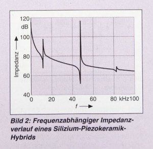
For example, micromechanical resonators excited by piezoelectric thin films and piezoceramically actuated actuator components can be modeled. In contrast to a mechanical excitation, this is done directly by the electric field quantities, so that the mechanical structural behavior can be calculated and various electrical characteristics can be derived, taking into account the electromechanical conversion. As an example, Fig. 2 shows the frequency-dependent impedance curve of a silicon diaphragm which is dynamically controlled by a hybrid piezoceramic.
Summary
The design, simulation and optimization of microsystem technology components is only possible by simultaneously considering different domains of problems. For example, optimization of micromechanical resonators can only be achieved if the static and dynamic properties are considered simultaneously, and the influence of excitation and sampling (electronics) is taken into account.
Therefore, the aim of future work is the development of adapted FE simulation models including the micro-technical requirements. Furthermore, experimental investigations, for example on test structures, are necessary to improve the described models.
Literature
Mikromechanik: Einführung in Technologie und Anwendungen
- Author: Prof. Dr.rer.nat. Stephanus Büttgenbach
- Paperback: 244 Seiten
- Publisher: Teubner Verlag, Stuttgart
- Edition: Nr. 1 (1991)
- Language: Deutsch
- ISBN-10: 3519130718
- ISBN-13: 978-3519130710
Micromechanics
“Micromechanics is concerned with the design, manufacture and application of three-dimensional mechanical structures and systems whose dimensions are so small in at least one dimension that fine mechanical shaping processes can no longer be usefully employed. Instead, micromechanics uses methods and materials from semiconductor technology that are generally suitable for creating structures in the micrometer range.” ~ Stephanus Büttgenbach
