MEMS
Resonant microsensors
TF Consulting offers specialized consulting and management services in high-tech sectors, with a particular focus on MEMS (micro-electro-mechanical systems) and microsystems technology. Our portfolio includes, among other things, product development services (PLM) for sensors and actuators:
- Development and Innovation: Support for the implementation of deep-tech and micromechanics solutions.
- Technology fields: Expertise in areas such as numerical simulation, software engineering, sensor technology, semiconductors, and data science.
How to create a good design
Developing silicon microsensors from scratch would require too much time and effort, and the accuracy and error rate would be unacceptable. That is why we offer our customers both analytical methods and highly powerful numerical simulation methods, including FEM and CFD. If we consider a simple micro–resonator, the desired operating range and sensor characteristic curve can, in principle, be estimated quickly. For complex calculations, numerical methods from mathematical approximation theory are well–suited.
Analytical description
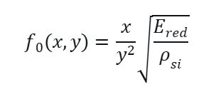
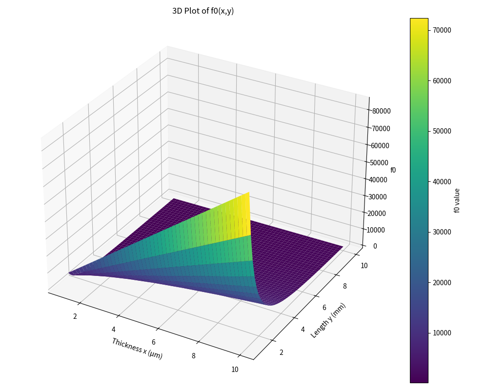
f₀(x, y) = (x/ y²) × √(E_red / ρ_si)where E_red = E_si / (1 – ν_si²) ≈ 1.696 × 10¹¹ Pa
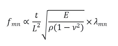
\lambda_{mn} is a dimensionless coefficient that depends on boundary conditions and mode indices (m,n).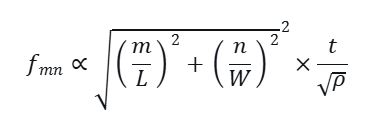
Key observations
- x-axis: thickness x (from 1 µm to 10 µm)
- y-axis: length y (from 1 mm to 10 mm)
- z-axis: f0 value (ranges from ~85 to ~85,300 in the plotted units)
The function increases linearly with thickness x and decreases strongly (as 1/y²) with length y. This behavior is typical for the fundamental resonance frequency (or similar quantity) of a thin beam or plate in MEMS structures.
Plot details
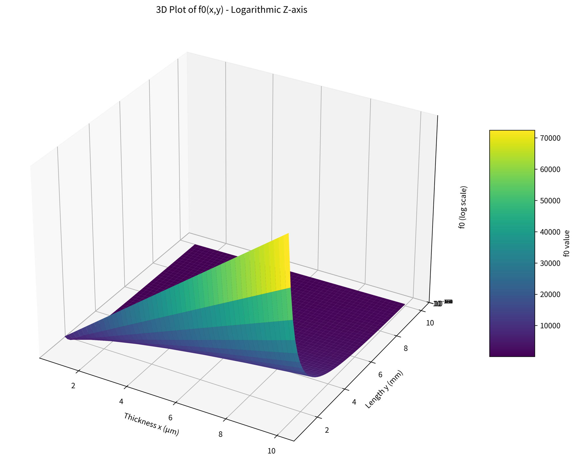
- X-axis: Thickness x (1 µm to 10 µm)
- Y-axis: Length y (1 mm to 10 mm)
- Z-axis: f₀(x,y) on logarithmic scale
This makes the strong 1/y² dependence much easier to visualize across the full range of values (roughly 85 to 85,000, i.e. 85 kHz resonance frequency).
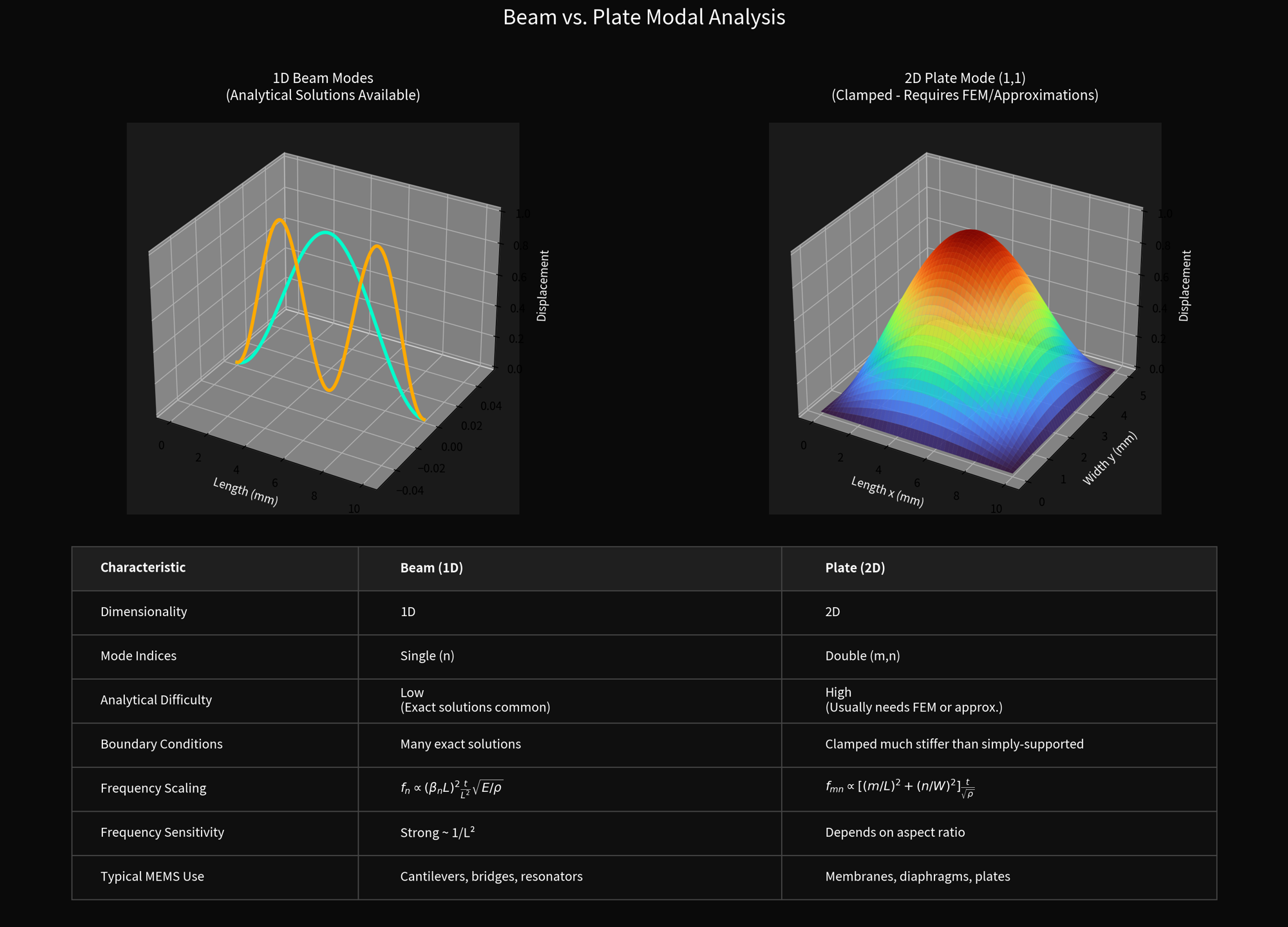
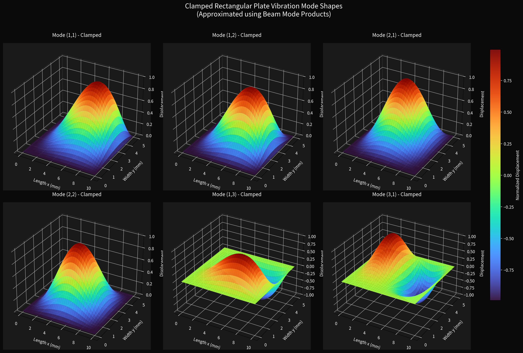
Modal Analysis
Beams (1D):
- Analytical solutions exist for many boundary conditions.
- Frequencies scale with (βnL)2tL2E/ρ(β_n L)^2 \frac{t}{L^2} \sqrt{E/\rho}
(β_n L)^2 \frac{t}{L^2} \sqrt{E/\rho}
Plates (2D):
- More complex; often require numerical methods (like FEM) or approximations.
- Two indices (m,n) for vibration modes.
- Clamped boundaries increase frequencies significantly compared to simply-supported.
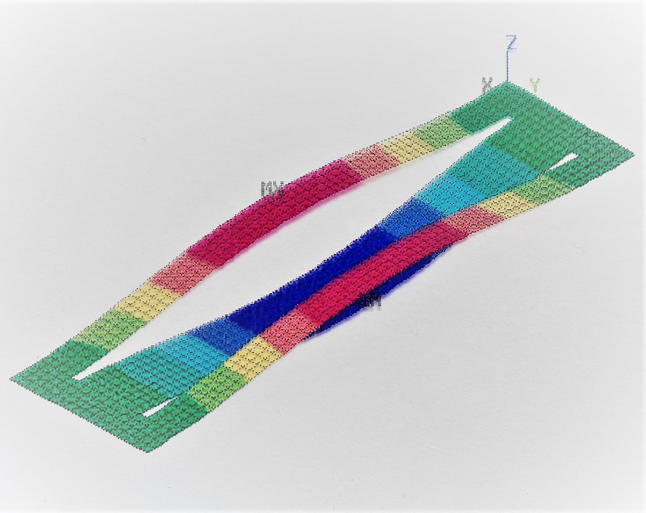
Cantilever Beam Mode Shapes
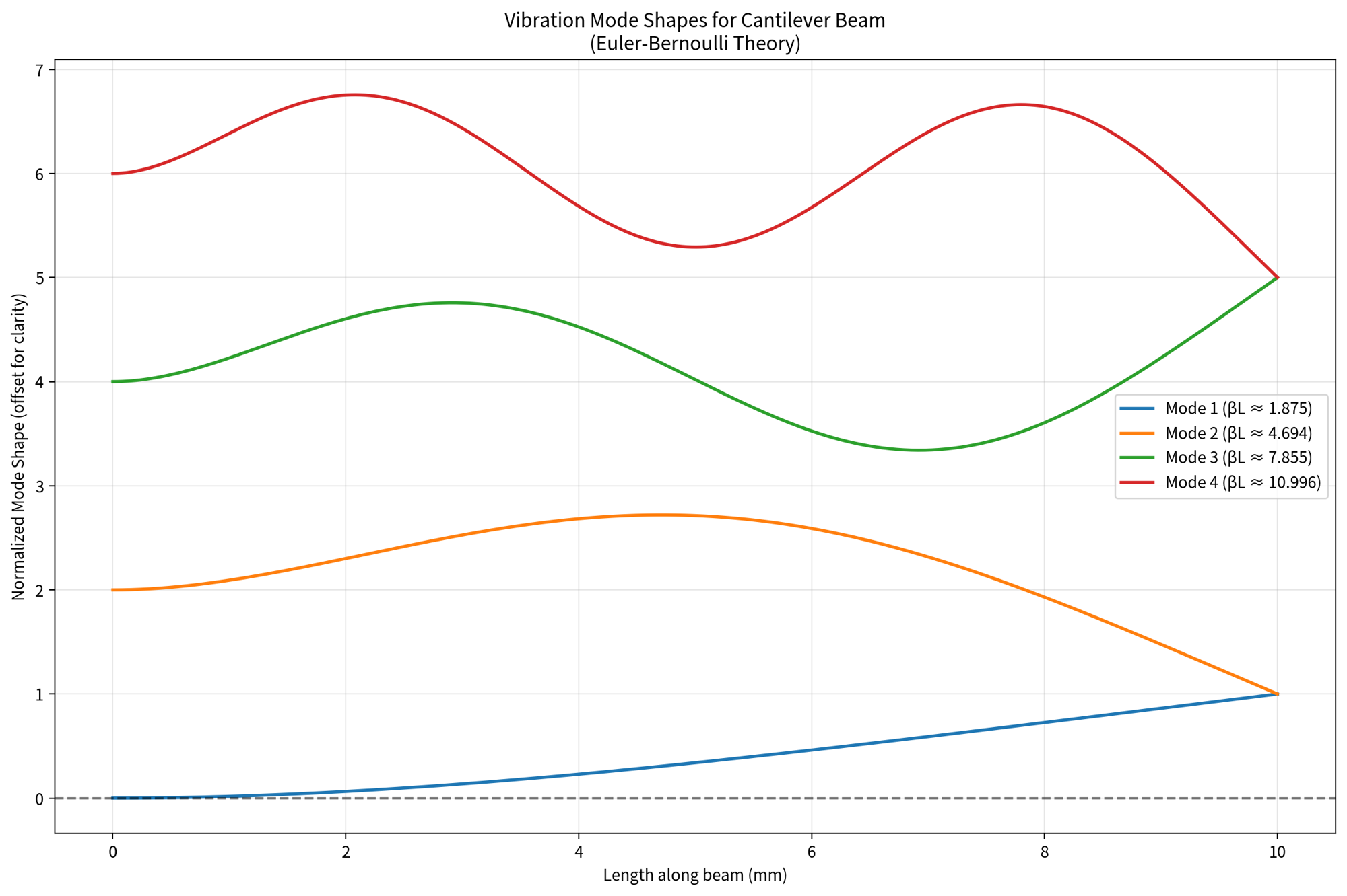
Key characteristics:
- Mode 1: Smooth bending, maximum deflection at the free end
- Mode 2: One node (point of zero displacement) along the length
- Higher modes: More nodes, higher curvature (and much higher frequencies)
Frequencies scale roughly as (βₙ)² × (thickness / length²) × √(E/ρ), where βₙ are the eigenvalues (1.875, 4.694, 7.855, …)
Vibration mode shapes
Micromechanical sensors
To optimize the performance of resonant silicon and quartz microsensors, a precise understanding of their internal behavior is required. Modeling and numerical simulation are necessary to achieve this within a reasonable amount of time. For simple resonator structures with ideal boundary conditions, analytical models can be used to accurately calculate their properties, assuming homogeneous and isotropic material behavior.
For more complex resonator structures, arbitrary boundary conditions, anisotropic and temperature-dependent material properties, as well as coupled field effects (multiphysics), the finite element method (FEM) and computational fluid dynamics (CFD) can be used to simulate the properties of resonant microstructures.
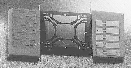
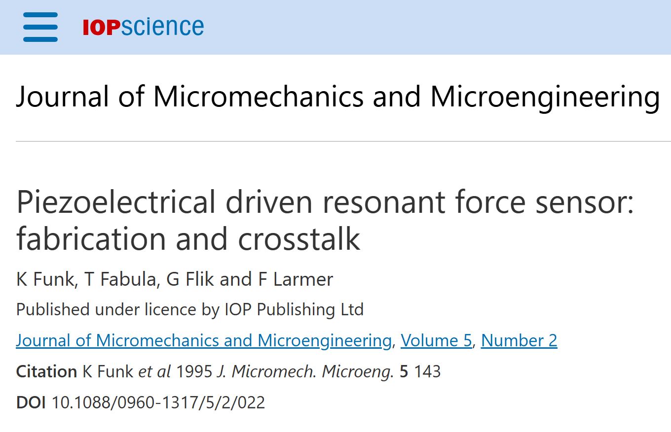
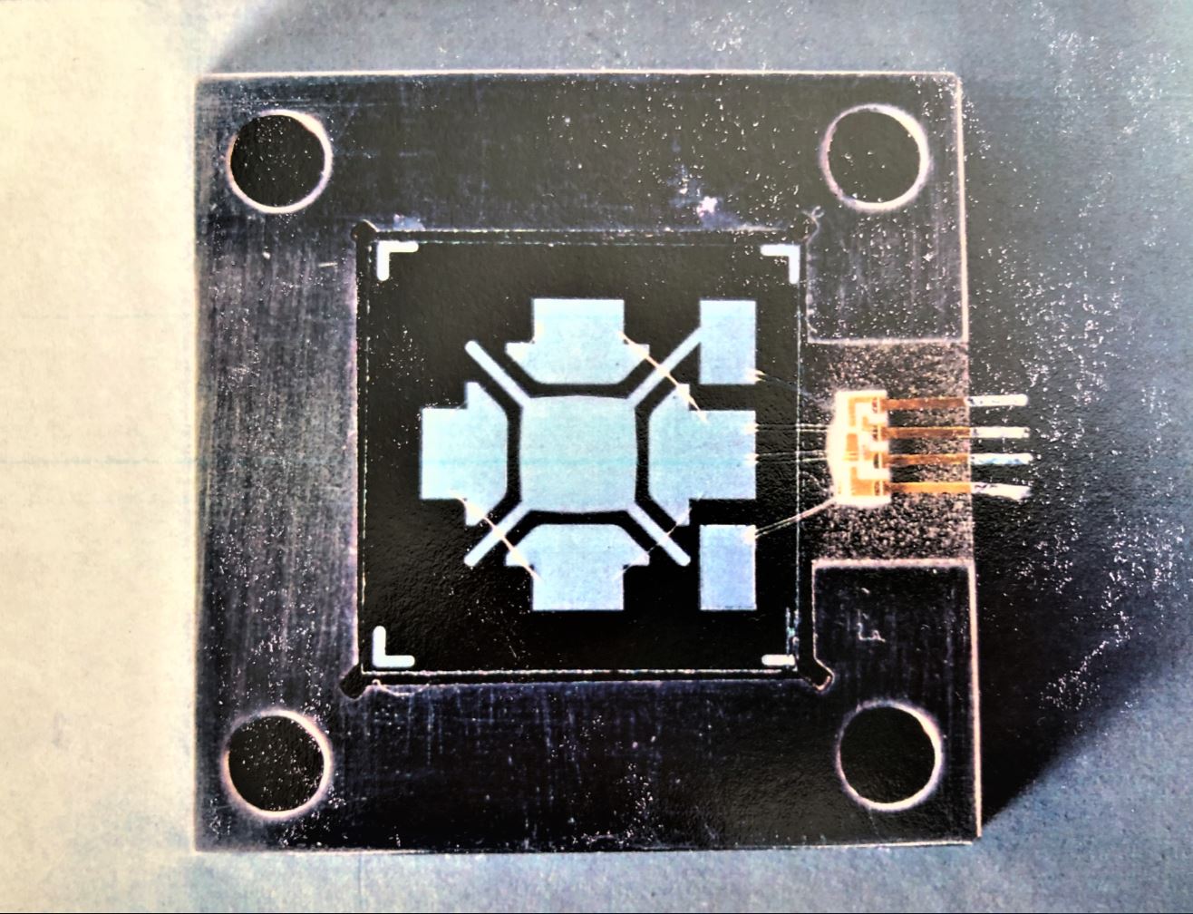
Piezoelectric layers
Focus areas of our Services
- Development & Implementation: Support from the initial idea through modeling to the implementation of microsystems technology within the company.
- Multiphysics Simulation: Use of computer–aided methods (such as FEM / CFD) to precisely calculate the behavior of micro sensors & actuators in advance.
- Cross-Industry Applications: Optimization of MEMS components for the defence and automotive industries (Automotive), the Internet of Things (IoT), and the general semiconductor industry
GitHub Repositories
- github.com/ThomasFabula/BMFT_FASENS
- github.com/ThomasFabula/Quartz-DETF
- github.com/ThomasFabula/piezoelectric_simulation
- github.com/ThomasFabula/Modeling-of-Resonant-Silicon-Microsensors
Patent
Testimonial
Retrospective